Sunday, 20 April 2014

FIN FET - part 3

Fin FET -> Field Effect Transistors: It is all about Gate Control of the Channel

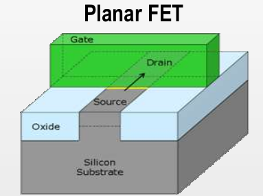
i)  Planar Fin FET = single gate

- Single gate channel control is limited at 20nm and below
- Increasing sub-threshold leakage
- Increasing gate leakage
- Decreasing mobility


ii) Fin FET = Multiple gate

- Better control of short channel effects
- Lower DIBL , drain induced barrier lowering and lower SS, subthreshold swing
- Higher ION/IOFF for fixed VDD, or lower VDD to achieve target ION/IOFF


Clear Advantages


Excellent short channel control leads to
– Lower leakage (lower DIBL drain induced barrier lowering and lower SS subthreshold swing)
– low threshold voltage  variability due to low channel doping
– Less variability caused by random dopant fluctuations
– Lower operating voltage -> 50% dynamic power savings

Additional Considerations
- Quantized widths (and channel lengths)
- Body biasing totally ineffective
- Higher parasitics
- Potential Self-Heating issues
- Thermal aspects of ESD can be an issue
- Degradation and aging: NBTI a bit worse than planar


 FinFET SRAMs The Good News
- Higher performance and lower leakage compared to planar
- Operates at lower Vdd than planar
- Good static noise margin at low Vdd
- Decent noise to signal ratio can be achieved (with a β=2 for example)
- Good (Low) Variability
- Read Margin and Write Margin distribution narrower than in planar

Resource : FinFETs & SRAM Design, Raymond Leung VP Engineering, Embedded Memories, April 19, 2013

FIN FET - part 2

Why Fin FET ?


The solution of the Vth leakage is create a new architecture whereby it is fully depleted devices for better short - channel control.


Fully depleted channel -> Steeper slope -> Target lower threshold voltage -> improve circuit speed


GATE DELAY :
 Circuits slow down as Vdd reduces
 Planar improves over previous node

  FinFET improves over planar, particular at low Vdd
                    FinFET can operate at lower Vdd, reducing active power >50%

FIN FET :
▸ Enables low Vdd operation and chip power savings
▸ Expected to be adopted as mainstream at 16-14nm

Challenges are in process control
▸ Wfin, Hfin
▸ Gate profile
▸ Junction, Strain...

Outlook 11-10nm and beyond ?
▸ FinFET using non-Si channels...SiGe, IIIV


Resource :
S. Biesemans, VP Process Technology & Strategy, FINFET FOR SUB-22NM TECHNOLOGY NODES

Friday, 18 April 2014

TCAD tools : Athena and Atlas

 Q : What is athena ?
 A : Athena is one of TCAD tools that used for MOS process simulation.This tool
      is under Silvaco.


Q  : How about Atlas ?
A  : Basically, atlas and athena has its own special link. It means that, atlas is a simulation for electrical and thermal behaviour of semiconductor devices.

Wednesday, 16 April 2014

FIN FET (14nm) - part 1


3D fin fet
Q : Why Fin fet is so special ?
A : Fin fet is actually is an improvement from traditional planar transistor. So, Fin fet has it's own speciality such as higher performance,lower leakage and has smaller layout area.Besides that,fin fet has lower Vdd and delay than a planar process.err... how to prove it ? okay,lets scroll down

.....

.....

.......


aha!


14nm finfet tech
FinFET can operate at lower Vdd ->  reducing active power >50%


Q: Why Fin Fet has higher performance rather than planar ?
A : Nowadays,most people talked about Metal Oxide Semiconductor [MOS] technology of the year because traditional planar CMOS has slowed down on scaling below 28nm node.Planar also has a greater leakage planar CMOS device as well as decreasing mobility (strained silicon helps)


Resource :
 http://www.dailytech.com/Samsung+Roadmap+Folding+4K+Display+Smartphones+Custom+64Bit+Cores+and+LPDDR4/article33698.htm